When last we left our discussion of soldering, we touched briefly on each of the basic topics concerning joining electronic parts together using a solder of some sort. Let’s do a short review of what soldering is all about:
• Soldering is the joining of two metal parts together with a similar metal with a similar melting point.
• Most things we are soldering together have a relatively high melting-point metal coated with a lower melting-point metal. In general, the metals to be joined are copper coated with a tin/lead mixture of solder. Typical is a copper wire soldered to a copper track on a PC board.
• Most all metals (solder included) “protect” themselves with a hyper-thin oxide barrier to prevent corrosion. Some sort of flux oxide remover is necessary to melt this oxide barrier to let the two metals “melt” with each other before the new joint has a chance to form the oxide barrier.

Let’s start off with a discussion of solder itself. We saw in Part 1 that common 60-40 (tin % to lead %) melts around 376° F while the less common 63-37 version melts at 361°. The problem is that if there is any movement of the 60-40 joint in this range (361°–376°), the joint will develop microcracks that will materialize in rotten weather at night over the mountains in turbulence.
To boot, our colleagues in Europe have banned the use of lead-based solder for health reasons. That forced a lot of us to go to some other system. Tin all by itself makes lousy solder. It doesn’t “wet” the parts being soldered to make a really good joint. Adding a bit of silver (3% or so) helped with the wetting, but an alloy of 96% tin, 2% silver and 2% copper was nearly as good a wetter as good old 60-40. I suspect that the EPA will be taking a good hard look at 60-40 solder sometime in the near future.
Yeah, I know, 96-2-2 solder is nearly 10 times the cost of 60-40 but then again, what is the cost to you of developing some really nasty problems if you’ve been using 60-40 with cracks over the mountains in the stuff. I’ve just been lucky. Try Jameco to get reasonably small amounts of 96-2-2 for a reasonable price.
Rosin flux is a super-cleaner. It works with all alloys of solder to clean oxide. Most of the prepackaged solders come with a core of flux, but if you’ve got a very old part or PC board with thick oxide, you may need a little help. Google “Kester #951” for a dozen sources from small pens to gallons (Amazon is a good source). Caution—flux is hygroscopic (attracts water). You may wish to wash your joint(s) with alcohol to remove the flux after soldering. 95% isopropyl works well, but you can use Jack Daniels if you don’t mind your radio having a Southern twang.
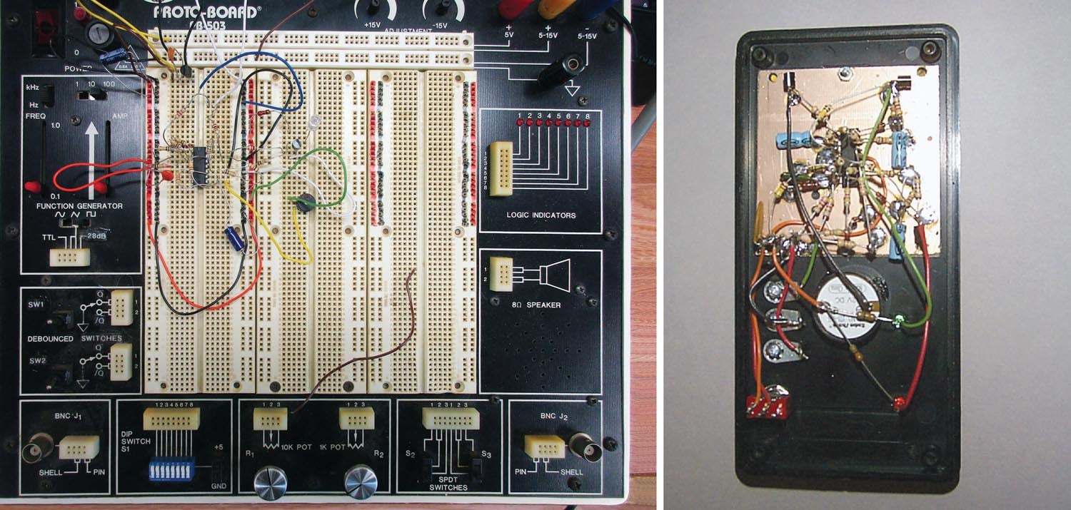
PC boards are how more than 95% of all circuits are made today. I wish to the holy St. Potluck that I could show you what I cut my teeth on in this business with vacuum tubes and big parts connected together with real thick copper wires with rubber insulation. The term rat’s nest easily comes to mind. The PC board is today’s answer to that mess, but there are a couple of things you should know about soldering parts onto a PC board.
The most common PC board is a relatively thin (64 mil) fire-resistant sheet of fiberglass that is bonded on both sides with a fairly thin (1 mil) coating of copper foil. The bonding is done with a relatively heat-resistant glue.
The PCB layout artist (that would be me) gets schematic information from the design engineer (that would be me) as to what components are going to be used, and the layout artist gets component information (sizes, diameters, etc.) from the components engineer (that would be me) and lays out the board in accordance with dimensions from the mechanical engineer (that would be me). The layout artist has a complete library of hole dimensions, lead separations and all that, and lays out the board so that everything fits in an area the size of the board.
In particular, the library has the diameters of the “pads” (circles that the components are going to be soldered to), diameters of the holes that the component leads are going to fit into and the outline of the part itself.
Here is the magic behind the curtain: From that board layout comes a set of files that tells the people who are going to make the board all this information about pad size, hole diameter, placement and all that. Through the magic of photography, the “board house” transforms those files into photographic images (Google “Gerbers”). The raw board is coated with “photosensitive resist” that is hardened with the image you want on the board, then the board is “flashed” with the image. Next, the board is dunked into resistant solvent, and the hard part stays and the rest of the resist is washed away.
Not so fast. Now the automatic drill, with at least six different drill sizes, is loaded up with your computer files and knows where to drill and what size to drill. Your board is drilled and sent back to the plating process. And this is the real magic behind the curtain. The entire board is dunked into a solution that adheres to the inside of the drilled holes. The drilled holes are put into a plating process that deposits regular hard copper into those holes. Now we have a hole on the top of the board, a hole on the bottom of the board and a tiny “barrel” of copper that joins the top and the bottom of those two holes.
Five more steps and we are done with this process.
Step 1: The board is dunked into a nasty acid that washes away all the uncovered copper, leaving only the resist-covered pads and traces. Then it is dunked into another solvent that washes the resist away.
Step 2: The board is run through a hot solder bath that plates a relatively thin layer of solder on all the copper surfaces (top traces, bottom traces, top pads, bottom pads and all plated holes between top and bottom holes). This leaves a tiny barrel of solder joining all the top holes to the bottom holes. This is nicknamed the PTH process (plated through holes).
Step 3: For almost all of us who have slightly shaky solder hands, a third photographic process lays down a coat of enamel paint (called a “solder mask”) over the whole board (top and bottom) that keeps the ham-handed from inadvertently joining two adjacent pads or traces.
Step 4: The board goes to a silkscreen (computer) process that lays ink down on the top side of the board so you know where to put your parts.
Step 5: Then your PC board house sends your completed board(s) from a domestic source that will make them for you for about $20 a board or an offshore source that will do them for about $5 a board (both in quantities of 20 or so). One domestic source specializes in prototype boards (www.oshpark.com) and will do them for about $10 a board, with a minimum quantity of three copies per board.
We’ve covered everything except the tools of the trade. One more column on soldering (and desoldering) tools, and we should be able to solder this puppy shut. Until then…Stay tuned…


