OK, this one is the witch of the bunch. You’ve had two months to download and read all the instructions for Circuitmaker/Traxmaker, and I’m sure you have committed the entire sections to memory. Funny, I taught this subject to my college classes for 30 years and half the class had some lame excuse: “The Padres were playing the Dodgers this week,” “the sorority mixer was this week,” and on and on. It’s OK, I understand. Just don’t jump from one figure to the next without getting 100% results, or you will be so far lost you will never catch up. Unless you start all over again and do it step by step and don’t move on until you “get it.” Sort of like building a homebuilt and missing Chapter 2.
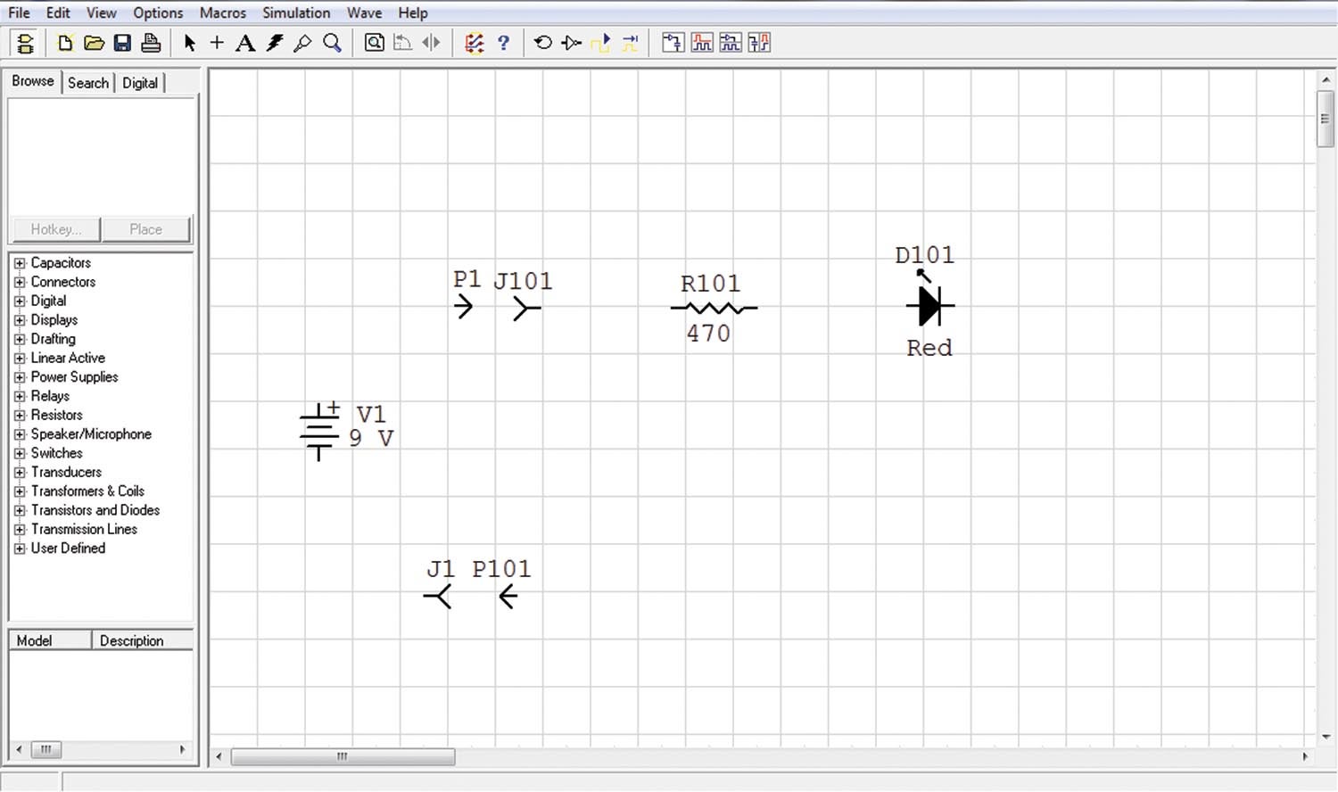
Figure 1 has all of the parts we talked about last month, and they were all pulled out of the parts library to the left of the main screen. You have taken V1 and P1/J1 into properties and told Circuitmaker that these were not parts on the PC board. On the other hand, J101 and P101 were never designed to be on a PC board, so you have to go in to their properties and tell them that their “package” is a “round 35/55” (a 55-mil diameter metal pad with a 35-mil drill hole in the middle). Don’t worry, all will be revealed.
Just an aside, in the “User Defined” section of the parts library, you will probably find all of the parts you need to do a full schematic for your own airplane: generator/alternator, lights and all the rest of it. Right there for the taking.
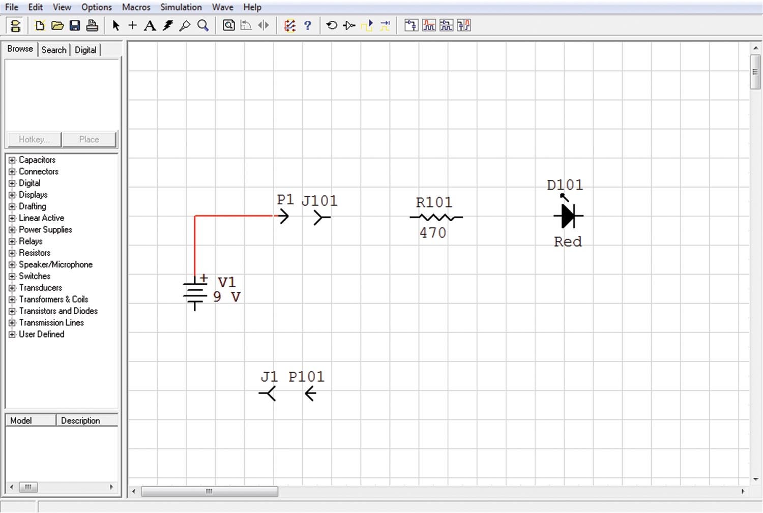
Figure 2 has all the parts arranged in a logical sequence. Power comes in from V1 to the left, goes through the battery-board interface P1-J101, through the current limiting resistor R101, through the LED D101, then out through P101-J1 back to the battery. Figure 2 also starts off the wiring commands with a connection from V1 to P1. When you run the mouse pointer near the (+) end of V1, a little red square comes on. If you drag that little square to the left end of P1, it shows a connection between V1 and P1.
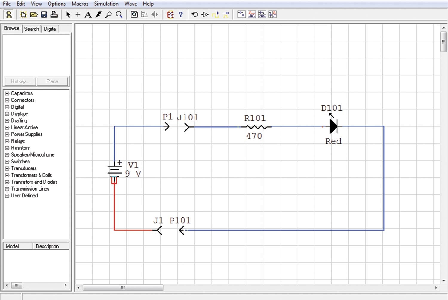
Figure 3 shows the whole circuit wired up. Click and drag, click and drag, and so on.
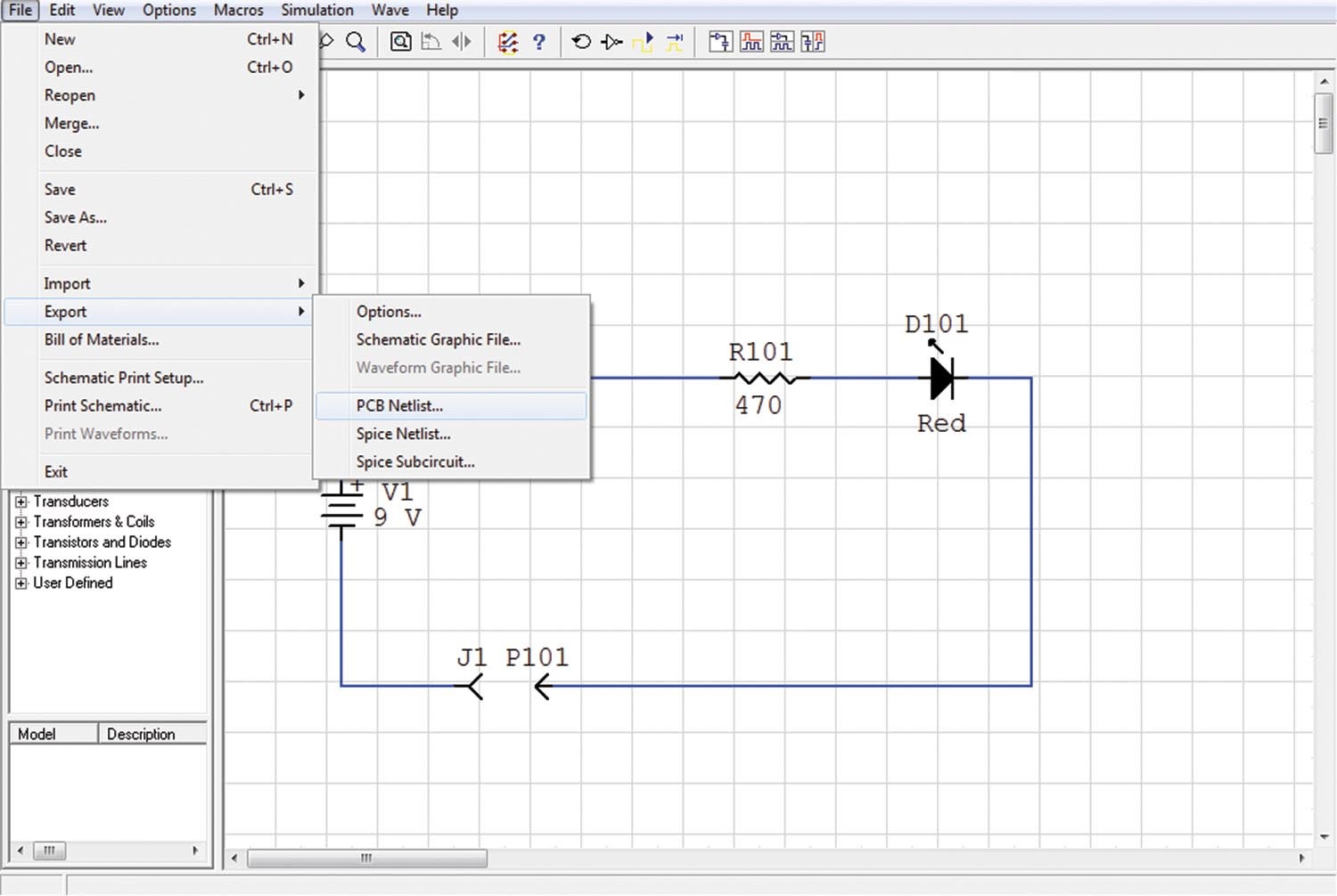
Figure 4 starts the translation from a schematic to a PC board. Under the left top corner “File” menu, we have “Export,” which brings up a submenu, “PCB Netlist.”
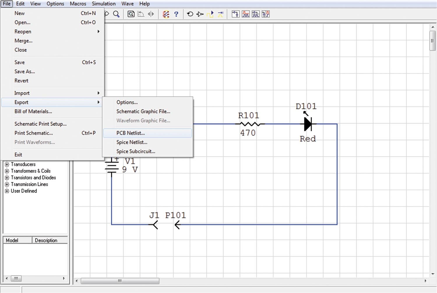
Figure 5 shows if we select “Export” and “PCB Netlist” and click on it, it brings up Figure 6.
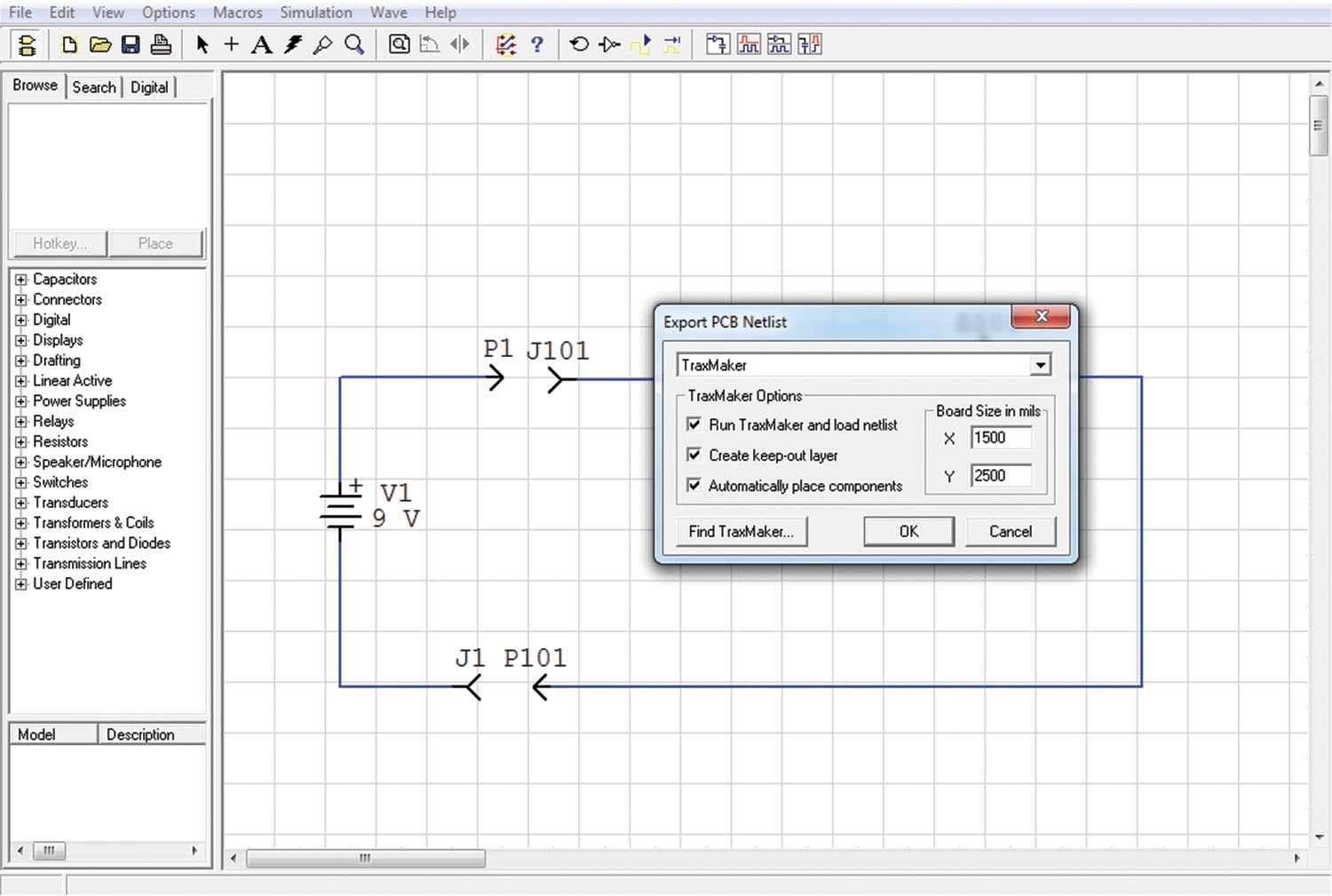
Figure 6 shows options for how I want to export the schematic. Yes, I want to export it to Traxmaker. I want all the goodies checked on the left, and now the question (on the right) is how big a board do I want to make. I’m pretty sure I can fit all this stuff on a 1.5×2.5-inch (1500×2500-mil) board, so I click OK and up comes Traxmaker.
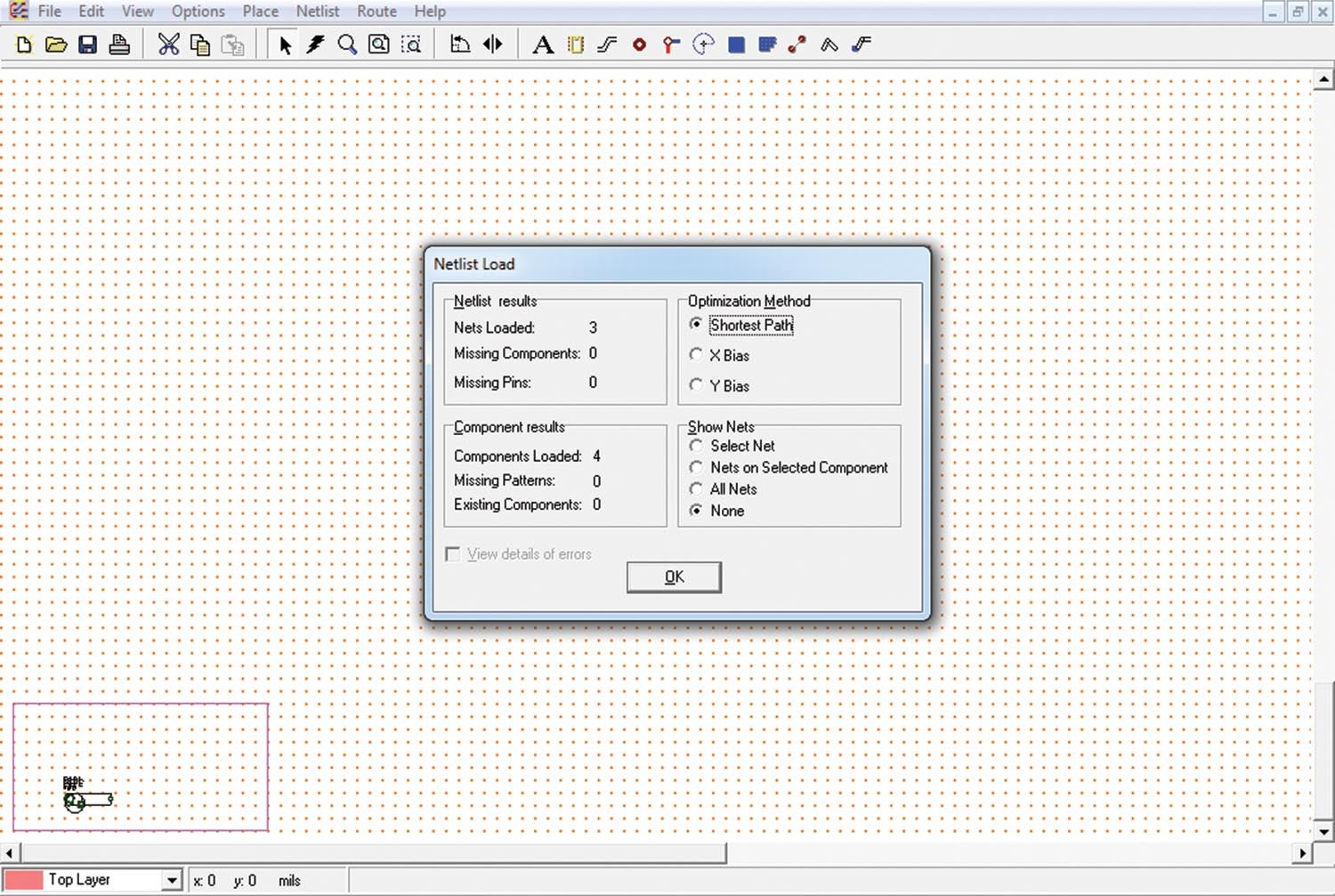
Figure 7 is the first thing we see in Traxmaker. See that little tiny rectangle in the lower left-hand corner with all those parts in a dogpile? That’s our PC board. The little square in the middle told us how many parts we brought in, any missing parts, how many “nets” (wires) we brought in and so forth.
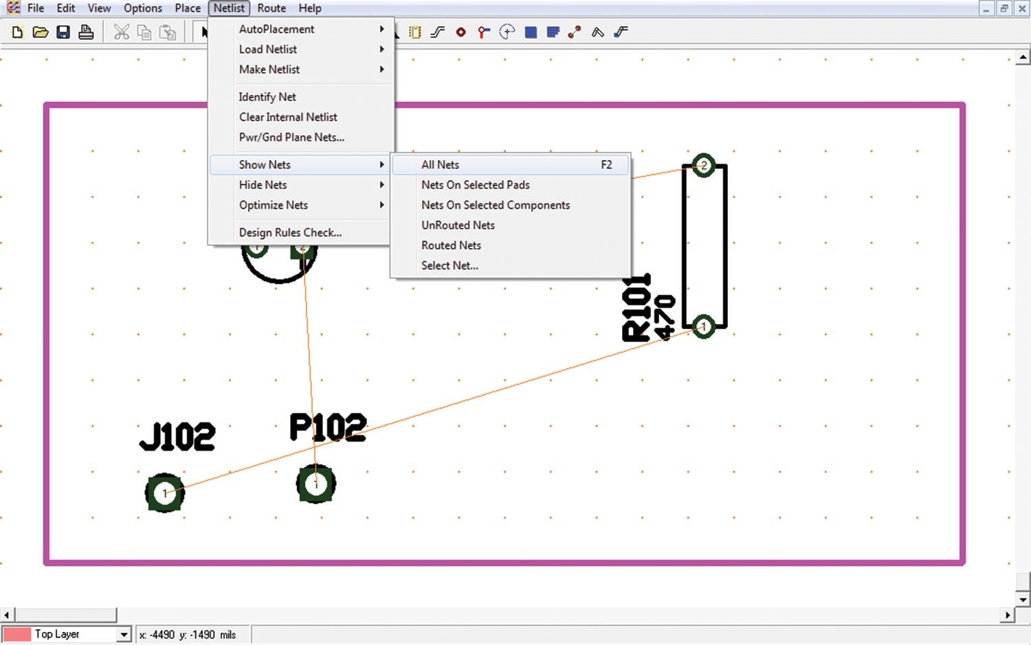
Figure 8 is the expanded (View) command from the top command list and all of the nets we had to connect (orange lines from part to part).
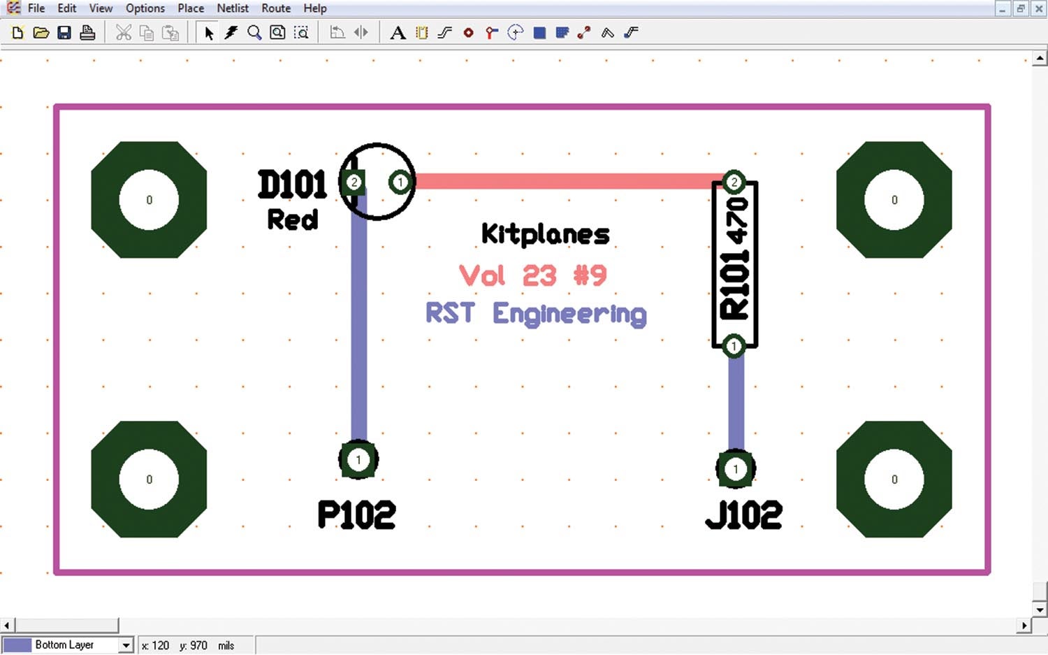
Figure 9 allows us to select which layer (top or bottom) we want to work with and what traces (trace command in the top command line). Traces on the bottom of the board are traditionally in blue and on the top of the board in red. This tradition is from the olden days when we did PCB layout photographically, and red and blue filters on the camera completely blotted out red from blue and vice versa.
Could I have made this PC board from all top or all bottom traces? Of course I could. Would it have allowed me to show you how to “register” (make sure that the top traces and the bottom traces mated)? Not at all.
Figure 9 also shows something that is most interesting. PC boards aren’t just shoved into an enclosure and expected to work. In this case we have some mounting holes in the corners of our board. They have metal on both sides of the board, so I made provisions for #4 screws. The “Holes” library at the top of the Traxmaker toolbar has most every size and shape of hole you will ever need.
So, you have just completed CIE 14a and CIE 14b, a two-semester college class in two short months. Next month, the final exam: Take the PC board we are going to design, put it into chemistry and see if we can come up with a “buzz-it” mag timer circuit board. Study for the exam and until then…stay tuned…


