That is what PC means, yes? No. It’s short for printed circuit. And the first attempts at making boards were actually made by spraying (“printing”) hot liquid copper onto a bakelite plastic sheet. The reliability with this method hovered somewhere between 0 and 1%. Not good.
After a few iterations, here is what we found works best: a fiberglass sheet about the thickness of a slice of cheese with very thin copper sheet bonded to the fiberglass with some really good heatproof glue. Then it’s run through a hydraulic press to firmly bond the copper to the cheese/fiberglass sheet. Next, we chemically dissolve the parts of the copper we don’t want in an acid bath. What remains is what we use to connect our circuit and to mount/fasten our parts.
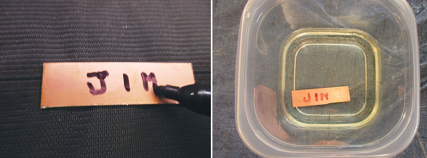
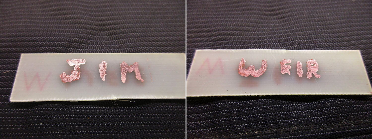
Allow me to illustrate a primitive method of doing this: I take a scrap of PC board material, write on it with a “permanent” marker and dunk it in muriatic (swimming pool) acid with a bit of hydrogen peroxide. The acid can’t eat through the marker ink, but in pretty short order (half an hour) it has eaten the copper from the fiberglass board. A splash of paint thinner then dissolves the ink and we have a copper pattern on the electrically nonconductive fiberglass sheet. We could, if necessary, make primitive circuit boards this way.
The next step up is to either hand-draw the circuit on paper or use a drafting program to draw the circuit on paper. Then we scan the drawing into a laser printer and print the circuit out with the printer. Why a laser printer? Because the “ink” (toner) in a laser printer is actually a plastic powder. We can melt this plastic ink onto a PC board with a plain-old clothes iron, and now we have a method of making multiple boards (although horribly time consuming) from a single drawing. And we can make more tomorrow (or next year) by simply printing more of the same pattern with the laser printer.
Let’s talk a bit more about this drafting program of which I speak. If your only object is to make your board in onesie-twosies, then almost any drafting program, including the freebies like SmartDraw, will do just fine. If you want to make either a lot of boards or just a more professional one or two boards for your own use, you will probably want to download the PCB program that we use here at RST Engineering from the April 2021 file in the HOG link at www.rstengineering.com.
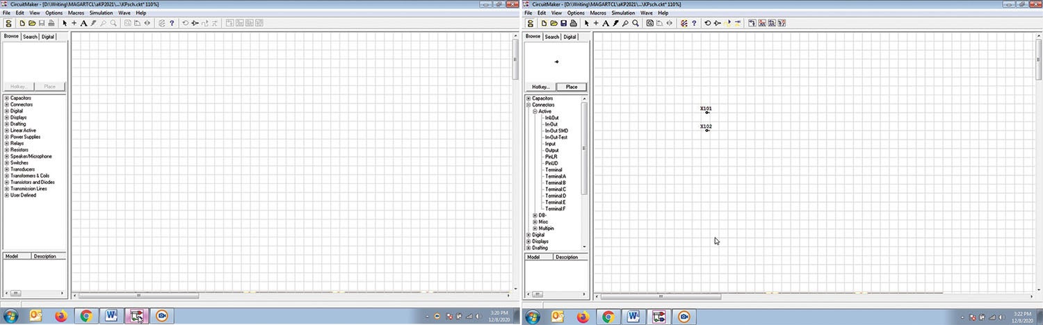
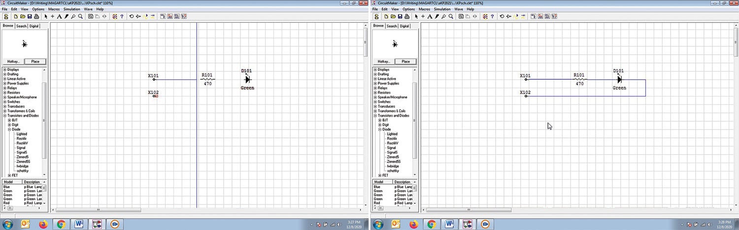
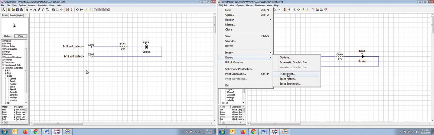
Let’s start out with a simple program that has (almost) all the elements of a much more complex project. All I want to do is hook a 9- to 12-volt external battery to the board and light a single LED when I hook up the battery. A simple schematic of such a board shows an LED, a resistor and a place to put wires from the battery connector.
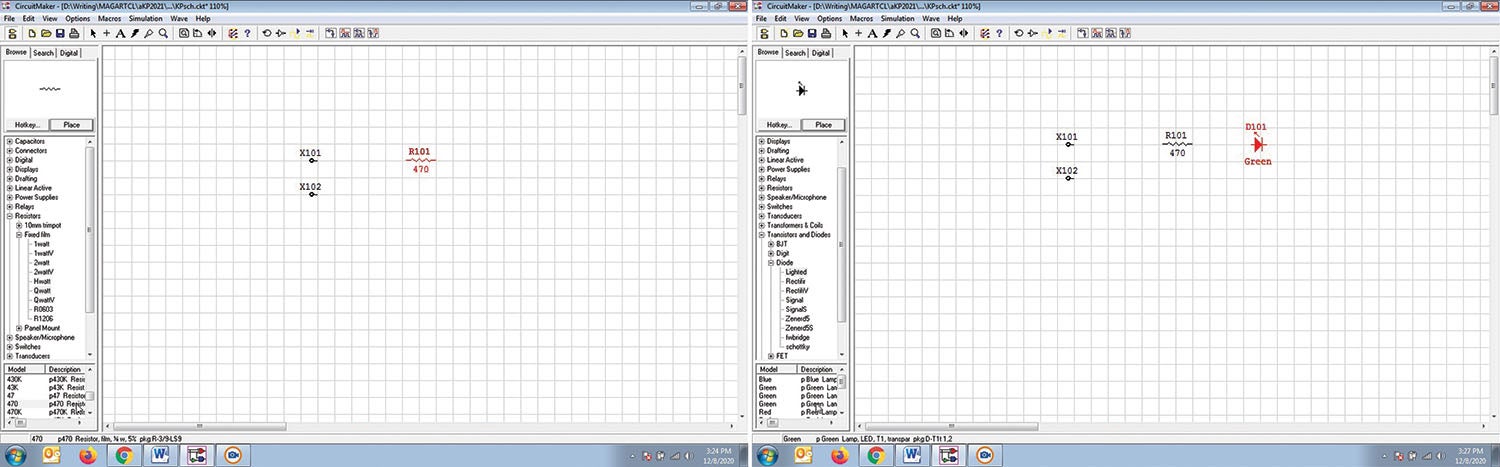
So let’s start by saying what we want. For example, I can have LEDs in dozens of configurations. The most popular (and the one I have the most of in my inventory) is a green LED in what is called the 3mm configuration. The 3mm configuration is standard across all manufacturers and we know a lot about it, including wire lead size, lead spacing, bulb diameter and all the rest of it. I only had to make one “package” for the 3mm LED no matter whether it is green, red, white, blue or yellow. Next, copy the original package four times and change only the color for the five colors. Then mass copy each of the colors with the “replace” function to change 3mm to 5mm and another copy to 8mm and so on.

The last steps are to print out the layout and etch it myself, or I send it out to have it etched professionally. This entire process took less than 15 minutes. The most complex board I’ve ever made (for a 10-channel audio selector panel) took me the better part of a day.
Similarly, a simple Ohm’s Law calculation shows that I can get by with a 470-ohm quarter-watt resistor, and we saw last month how to make resistor packages. The battery connector uses AWG 24 wire and we know what diameter #24 wire is (20 mils or 0.020 inch). That’s all the stuff we need to know to make our board, except for the size. Being a simple board, how about 1×0.5 inch, and those numbers are picked right out of the air (what engineers call rectorandom design).
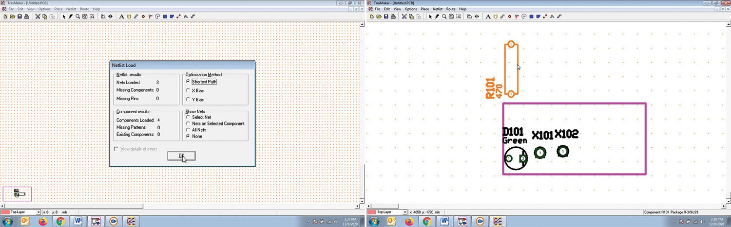
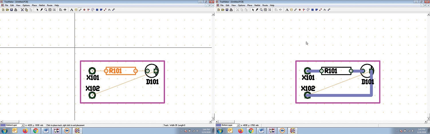
The images show the progression from conceptual thought to something that can be made in individual boards or by the millions, no changes. But note the change I made on the last image. Traditionally, all the copper wires (traces) on the bottom side of the board are in blue, and all the parts on the top or component side of the board are in black. The blue traces will be done in copper and the black top side will be in white ink. All the holes for the parts will be done in copper also. But what happens if I want to use the copper on the top side of the board? Easy. Just modify the color of the trace(s) that you want to change to red, and those will come out in copper on the top side of the board.
Now this is important as it makes a big difference on how you assemble the board: By dint of powdered bat wings and eyes of newts, the PCB manufacturing folks have figured out a magic way to drill the holes for the components to fit into, and then they copper plate the holes connecting the bottom component “pads” with their corresponding pads on the top. No need to solder both bottom and top pads; it’s been done for you.
This is a trivial board. Next month we’ll delve into the subtle details of how to make the battery charger board and how we can get the manufacturing part done for a very few dollars and not have to mess around with swimming pool acid and laser printouts. Until then…Stay tuned…


Excellent, Professor Jim!
Looking forward to next month!
Muriatic acid instead of Ferric Chloride? I might try this next time I etch a board.
Comments are closed.